


Initialising ...
Initialising ...
Initialising ...
Initialising ...
Initialising ...
Initialising ...
Initialising ...
Schaffer, M. J.*; Snipes, J. A.*; Gohil, P.*; de Vries, P.*; Evans, T. E.*; Fenstermacher, M. E.*; Gao, X.*; Garofalo, A. M.*; Gates, D. A.*; Greenfield, C. M.*; et al.
Nuclear Fusion, 51(10), p.103028_1 - 103028_11, 2011/10
Times Cited Count:35 Percentile:80.59(Physics, Fluids & Plasmas)Experiments at DIII-D investigated the effects of ferromagnetic error fields similar to those expected from proposed ITER Test Blanket Modules (TBMs). Studied were effects on: plasma rotation and locking; confinement; L-H transition; edge localized mode (ELM) suppression by resonant magnetic perturbations; ELMs and the H-mode pedestal; energetic particle losses; and more. The experiments used a 3-coil mock-up of 2 magnetized ITER TBMs in one ITER equatorial port. The experiments did not reveal any effect likely to preclude ITER operations with a TBM-like error field. The largest effect was slowed plasma toroidal rotation v across the entire radial profile by as much as 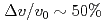 via non-resonant braking. Changes to global
  ,
,  and
and  were
were  3 times smaller. These effects are stronger at higher
  and lower
  . Other effects were smaller.
 -ray irradiation
Oshima, Takeshi; Onoda, Shinobu; Hirao, Toshio; Takahashi, Yoshihiro*; Vizkelethy, G.*; Doyle, B. L.*
AIP Conference Proceedings 1099, p.1014 - 1017, 2009/03
Metal-Oxide-Semiconductor (MOS) capacitors were made on both n- and p-type Si substrates (n-MOS, and p-MOS). These MOS capacitors were irradiated with -rays at a dose of 6.3 kGy (SiO ) at room temperature. The capacitance-voltage characteristics for MOS capacitors were measured before and after irradiation. The flat band shift for n-MOS and p-MOS capacitors due to -ray irradiation was -12.3 V and -15.2 V, respectively. As for the generation of interface traps, the values for n-MOS and p-MOS capacitors were estimated to be 0.5
 10
10 and 1.710/cm
 , respectively. Transient Ion Beam Induced Current (TIBIC) obtained from these MOS capacitors were compared before and after -ray irradiation. For n-MOS capacitors, the peak height of TIBIC signals decreased after -ray irradiation. On the other hand, the peak height of TIBIC signals for p-MOS capacitors increased after -ray irradiation. The applied bias dependence of the peak height of TIBIC signals for MOS capacitors irradiated with -rays can be matched to that for ones before -rays irradiation by shifting the voltage by -13 V for n-MOS capacitors and by -15 V for p-MOS capacitors. These voltage values are in good agreement with the flat band voltage shifts due to -ray irradiation. Since flat band shift occurs due to the generation of positive charge trapped in gate oxide, the change in TIBIC signals observed for MOS capacitors due to -ray irradiation can be interpreted in terms of positive charge generated in oxide.
